
Our research is driven by the thrilling prospect of discovering and manipulating new states of matter. This endeavor focuses on exploring the complex interactions among various elements, including reduced dimensionality, wavefunction topology, electron-electron interactions, relativistic spin-orbit coupling, and key symmetries.
In our group, materials of Interest include (but not limited to)
Scanning Tunneling Microscopy (STM) is an advanced surface analysis technique that revolutionized our understanding of materials at the atomic scale. Developed in the early 1980s by Gerd Binnig and Heinrich Rohrer, who later received the Nobel Prize for their work, STM operates on the principle of quantum tunneling. By positioning an atomically sharp, conductive tip extremely close to a sample surface (typically within a few angstroms), and applying a bias voltage between them, electrons are allowed to tunnel across the vacuum gap. The resulting tunneling current is exponentially sensitive to the distance between the tip and the sample, enabling the system to detect minute changes in surface topography and local electronic structure with atomic resolution.
1. Topographic Images. In constant current mode, the STM tip is moved laterally across the sample at a fixed bias voltage while a feedback loop adjusts its vertical position to keep the tunneling current constant. The recorded tip height variations are then translated into a topographic image of the surface. Tunneling current is dependent on tip sample separation as well as the integral of DOS from Fermi level to the bias voltage applied. For a sample with homogeneous DOS, the trajectory of the Z piezo walker corresponds to the real physical corrugation of the sample surface. This method is highly effective for mapping surface morphology, revealing atomic lattice structures, step edges, vacancies, and other defects.
2, Differential conductance (dI/dV) spectrum. Beyond mere topograph, STM can probe the electronic signals of a material through spectroscopy both in occupied and unoccupied states. By positioning the STM tip at a specific point on the sample and sweeping the bias voltage at a constant height (feedback loop off), one can record the dI/dV curve, which is directly proportional to the LDOS at the energy corresponding to the applied bias, with lock-in bias voltage modulation applied. These spectra provide insight into the local density of states (LDOS) of the material. Features such as energy gaps, resonances, and localized states become evident in the dI/dV data.
3, Differential Conductance (dI/dV) mapping. Mapping the LDOS spatial distribution as a function of energy creates a ‘3D’ DOS map, where ‘3D’ corresponds to the X and Y positions on the sample and the energy level. Extracting single layer (dI/dV map) at desired energy provides information of the spatial LDOS distribution at specific energy. Additionally, application of Fourier transform (FT) to the dI/dV maps can convert the DOS signals from real space to frequency space (or q-space), revealing periodicities and scattering vectors in the material.
Molecular beam epitaxy (MBE) is an advanced thin film deposition technique that enables the epitaxial growth of high-quality crystalline layers with atomic precision. In an ultra-high vacuum environment, beams of atoms or molecules generated from heated effusion cells are directed towards a heated substrate, where they condense to form well-ordered layers. This method allows for precise control over the composition, thickness, and doping of the layers, making it an indispensable tool for fabricating semiconductor heterostructures, quantum wells, and superlattices. With real-time monitoring techniques like reflection high-energy electron diffraction (RHEED), MBE not only achieves excellent material quality with low defect densities but also provides critical insights into the growth process, paving the way for innovations in nanoelectronics, optoelectronics, and quantum devices.
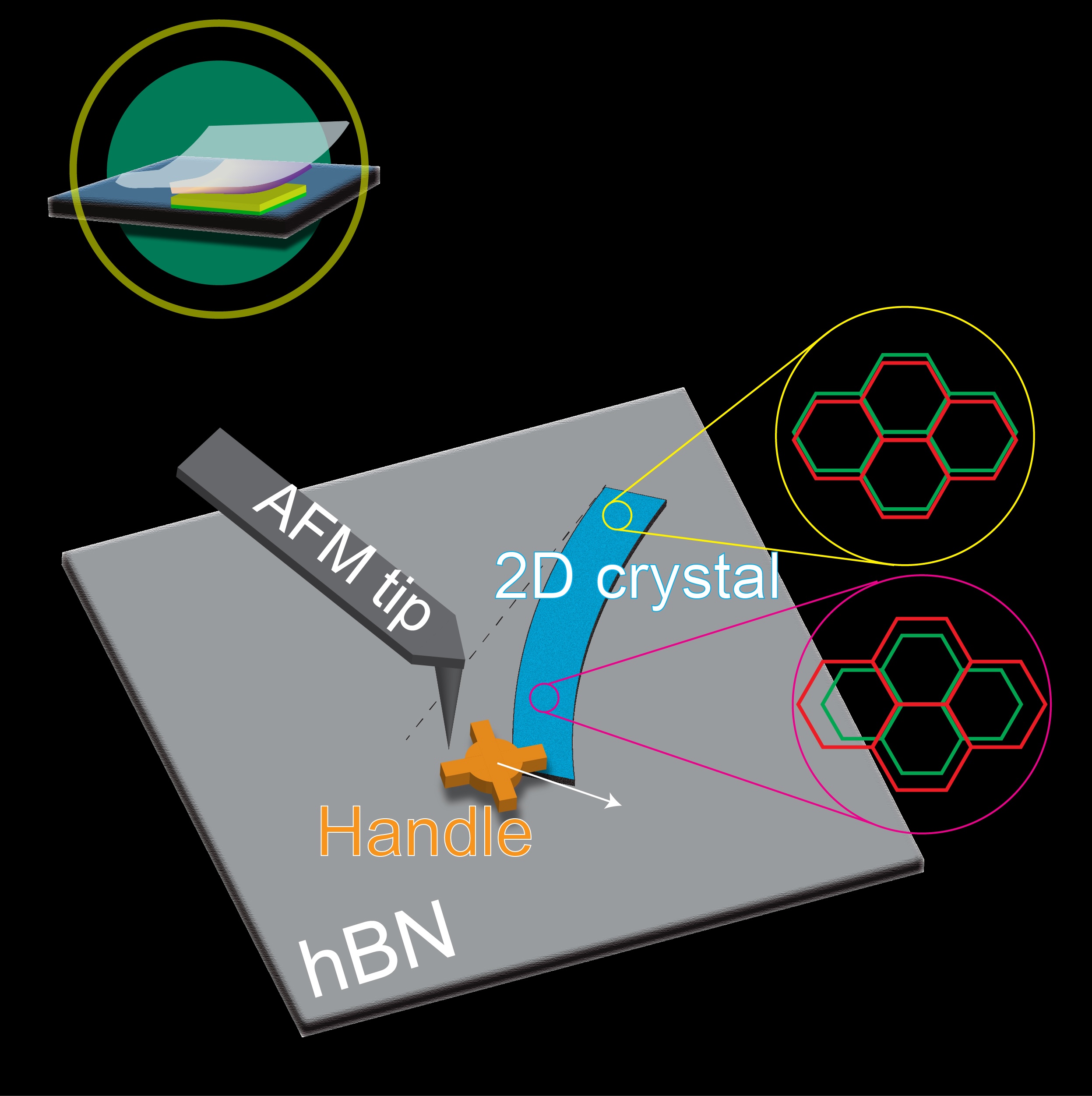
Co-laminated nanodevices, constructed through the precise layering of nanoscale films and structures, have emerged as a transformative platform in the realm of STM research. Their highly tunable interfaces and integrated functionalities allow researchers to probe local electronic and structural properties with enhanced resolution and specificity. These devices not only serve as sophisticated subjects for investigation—revealing quantum behaviors and interfacial phenomena—but also as potential tools to augment STM performance through engineered surface properties. This synergy between colaminated nanodevices and STM paves the way for deeper insights into nanoscale material science, enabling advances in nanoelectronics, catalysis, and sensor technologies.